From OLED Deposition to a Universal Thin-Film Platform: A Conversation with UVJC CEO Chandran Nair
We sat down with UVJC CEO Chandran Nair to talk about the evolution of vapor jet printing from its OLED roots into a broader thin-film technology platform, the team building UVJC’s future in Singapore, the launch of NovaJet and the opportunities ahead.
Innovation rarely follows a straight line. A technology developed to solve one challenge can sometimes reveal possibilities far beyond its original purpose.
That is the story behind Universal Vapor Jet Corporation, or UVJC.
Vapor jet printing traces its roots to UDC’s work in OLED. Originally known as Organic Vapor Jet Printing, or OVJP, the technology was developed as a novel, maskless and solvent-free approach to manufacturing large-area OLED displays, including OLED TVs. The work began as part of UDC’s R&D efforts in New Jersey, and in 2020, UDC established OVJP Corporation in Silicon Valley to advance commercialization of the technology, mainly for OLED TVs.
As the technology advanced, so did its possibilities. Its precision, flexibility and potential applicability to a broader range of materials pointed to opportunities beyond OLED and prompted UDC to explore how vapor jet printing could be applied to new materials, applications and industries.
That broader vision gave rise to Universal Vapor Jet Printing, or UVJP, reflecting the technology’s evolution from an OLED deposition technology into a broader thin-film platform. It also laid the foundation for UVJC. In late 2024, UDC announced plans to establish the new company in Singapore, and in October 2025, UVJC officially opened its global headquarters and R&D center.
Today, UVJC is taking that platform into new territory. Its first commercial system, NovaJet, is designed to give researchers and engineers a way to explore advanced materials, develop processes and validate applications, helping bridge the gap between laboratory discovery and potential commercialization.
Q: Chandran, let’s start with the evolution. UVJP began with UDC’s work in OLED. How did that become UVJC?
Chandran: The technology has a long history within UDC, starting with our academic team led by Professor Steve Forrest. What we now call Universal Vapor Jet Printing grew out of OVJP, or Organic Vapor Jet Printing, which UDC originally developed to address some of the manufacturing challenges associated with large-area OLED displays.
Over the years, UDC made significant advances in the technology. But the market around us was also changing. While UDC continues to see a long-term opportunity for OVJP in large-area OLEDs, the display industry increasingly directed near-term capital investment toward OLED IT capacity. UDC began asking a broader question: What if the technology developed for OLED could be applied to entirely different materials and manufacturing challenges?
That really set the stage for UVJC.
The focus expanded from a technology developed principally for OLED deposition into a platform with potential across multiple industries. That thinking also led us to Singapore, where we could build the next phase of the company in a major technology and advanced manufacturing ecosystem, closer to many of the customers, partners and markets we want to engage.
Q: And is that broader vision what prompted the change from OVJP to UVJP?
Chandran: Exactly. The change in name reflects the change in scope.
The “O” in OVJP stood for “Organic” because the technology originated with OLED. But as we explored the underlying capabilities more deeply, the technology showed potential applicability to a much broader range of thin-film materials and processes.
Universal Vapor Jet Printing better represents what we are building today: a technology platform rather than a solution for a single application.
Importantly, we are not walking away from the OLED foundation. UVJC is building on years of UDC innovation and applying those capabilities to new opportunities.
UVJC is the next chapter of that story. Our focus now extends to areas including semiconductors and electronics, life sciences and renewable energy.
Q: Tell us about the UVJC team. What have you built in Singapore?
Chandran: We’ve built a multidisciplinary team with a clear objective: to translate a powerful technology platform into solutions for real-world materials and manufacturing challenges.
Our Singapore headquarters brings together expertise across process and product engineering, software, electronics and mechanical engineering. We also have R&D, laboratory and prototype manufacturing capabilities within the facility.
That breadth of expertise is important because these are not simply equipment problems or materials problems. You need to understand the material, the process, the application, the system and, ultimately, what it will take to make the approach commercially relevant.
Singapore gives us an excellent environment for that work, with a strong advanced-manufacturing and innovation ecosystem, a deep talent base, and organizations such as the Singapore Economic Development Board and A*STAR that can help foster collaboration.
Ultimately, it is about bringing together the people, capabilities and technology to turn potential into practical applications.
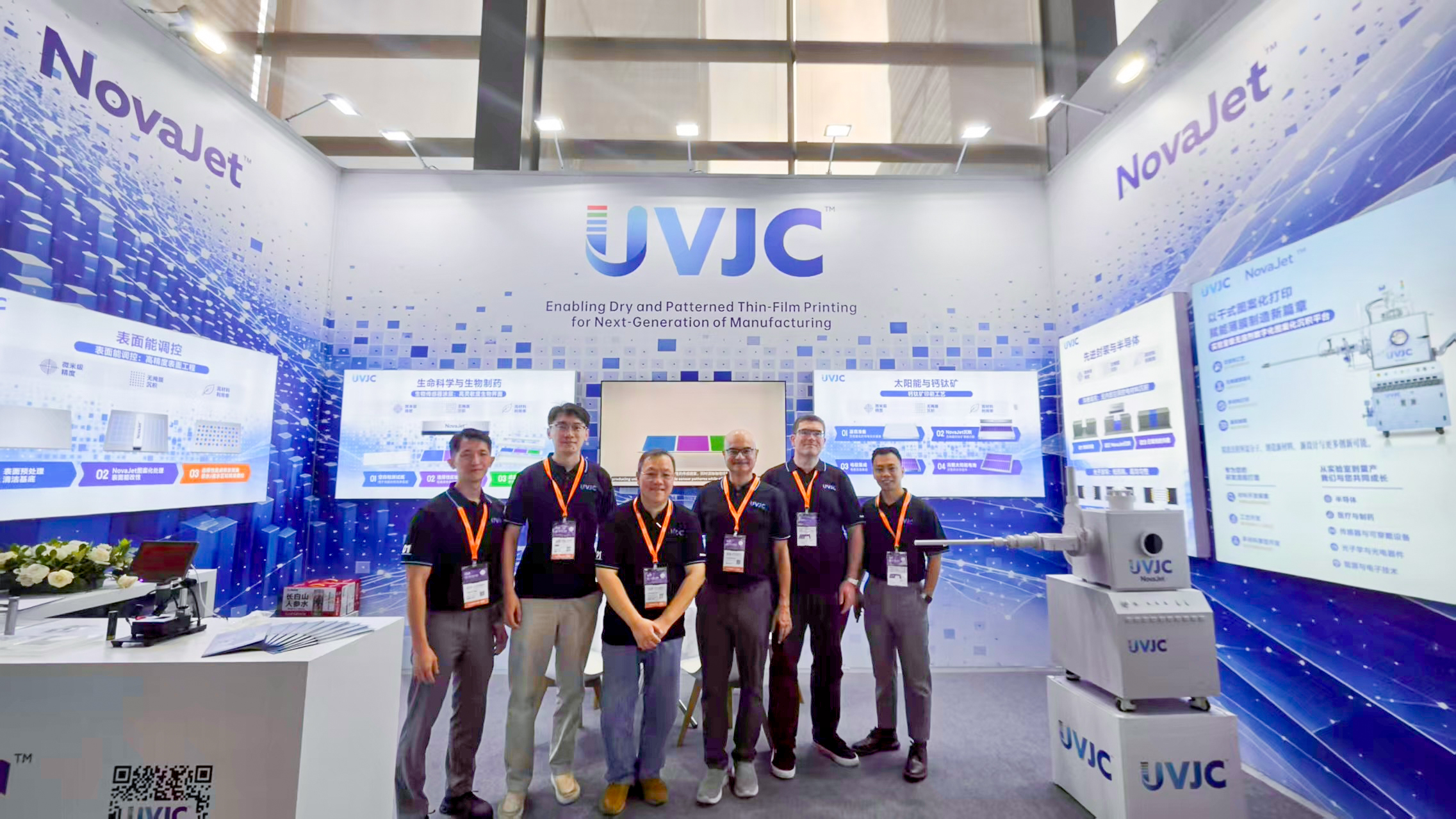
UVJC leadership and team members showcase the company’s first commercial system, NovaJet, at WESEMiBAY 2026 in Shenzhen, China.
Q: That brings us to NovaJet. What exactly is it?
Chandran: NovaJet is our first commercial system built on the UVJP platform. It is a laboratory-scale tool, designed to let materials scientists, process engineers and researchers put UVJP to work on their applications.
To understand what it does, it helps to understand how UVJP works. The material is evaporated into an inert carrier gas, shaped into a narrow, collimated jet, and written directly onto the substrate through a precision nozzle. The pattern is defined by where the nozzle moves, not by a physical mask. The whole process is fully dry: no solvents, no inks, no drying or curing step.
NovaJet packages that capability in a system that a research group or development team can use day to day. It handles a range of thin-film material classes, including organic small molecules, polymers and metal oxides, and can deposit them in digitally defined patterns at low temperatures, opening the technology to substrates that may not tolerate higher-temperature conventional processing.
One of the hardest steps in advanced materials development is getting from an interesting result in the laboratory to a process that can be manufactured. NovaJet is built for that step. It lets a customer answer the fundamental questions in order: Can this material be deposited the way we need it? Do we get the structure and properties we want? Does the process repeat? And if it works, what would it take to scale?
So NovaJet is about discovery and validation, and it creates a pathway from idea to experiment to validated process and, where it makes sense, toward manufacturing. That is why it is the first step in the broader UVJC strategy, not the whole of it.
Q: What differentiates UVJP from other deposition and patterning technologies?
Chandran: Four things, and each of them has a practical consequence.
First, it is solvent-free. Most thin-film processes outside the vacuum world, whether spin coating, slot-die or inkjet, start by dissolving the material in a solvent. That brings residual solvent, drying steps, and compatibility considerations for the layer underneath. UVJP deposits material directly from the vapor phase, so those issues do not applies, while also opening the door to materials that may not have a suitable solvent.
Second, it is maskless and digitally patterned. The pattern lives in software, not in a shadow mask or a photolithography step. That means no tooling cost, no mask alignment, and design changes that can be made in minutes rather than weeks. For a research team iterating on a device architecture, that changes the pace of work completely.
Third, it is low temperature. Because the substrate does not need to be heated, we can deposit onto polymers, flexible substrates, finished devices and heat-sensitive materials, including many that matter in life sciences.
Fourth, it is multi-material. The system can deposit more than one material through the same process, which makes it possible to create layered or graded films in a single run rather than through a sequence of separate steps.
If you look at the established processes, each offers different capabilities and trade-offs. Spin coating is solvent-based and cannot directly pattern. Inkjet can pattern, but requires materials that can be formulated into a printable ink. Physical and chemical vapor deposition are dry processes, but typically require additional patterning steps. UVJP brings these capabilities together: dry, digitally patterned, low temperature and multi-material in one process.
I would still describe UVJP as complementary to existing manufacturing, because in most cases it will sit alongside other steps rather than replace them. But where that combination of properties is the bottleneck, there is not really another way to do it, and that is where we are concentrating.
Q: Where are you focusing UVJP today?
Chandran: We are focused on three areas: semiconductors and electronics, life sciences, and renewable energy. They look very different, but in each one the problem has the same shape. Someone needs a functional material placed precisely where it is needed, with tight control over the process, on a surface that is sensitive to solvents, heat or both.
In semiconductors, the near-term opportunity is in advanced chip packaging, where the industry is integrating more dies into smaller spaces and needs new ways to deposit patterned functional materials onto finished devices without masks and without damaging what is already there. The low-temperature, direct-write capabilities of UVJP are well suited for these types of requirements.
In life sciences, the interest is in functional coatings on medical devices and in pharmaceutical applications, where being solvent-free matters a great deal. You can deposit an active ingredient or a polymer coating with no residual solvent and at temperatures that preserve the material. Those capabilities can be particularly valuable for materials and applications that are sensitive to conventional processing methods.
In renewable energy, we are looking at areas such as solid-state battery electrolytes and organic photovoltaics, where the ability to lay down thin, uniform, patterned layers of materials that are hard to process from solution could enable new approaches to device design.
The applications are diverse, but the approach is disciplined: identify where the capabilities of UVJP address a real materials or process challenge, prove it with the customer, and then build from there.
Q: How do you determine whether UVJP is the right fit for a particular application?
Chandran: We start with the problem, not the equipment.
A customer may come to us with a material, a substrate, a device architecture or a manufacturing challenge. The first question is: Can UVJP help solve this problem?
That’s where proof-of-concept work becomes important.
We work with the customer to understand the requirements and determine whether UVJP provides the capabilities they need. If the initial work is successful, the next step is further process development and validation.
That approach allows us to stay focused on applications where UVJP can deliver value, while building a deeper understanding of what the platform can do.
Q: Looking further ahead, how might AI change the way a platform like NovaJet is used?
Chandran: That’s an area we’re very interested in.
AI and machine learning are opening new ways to explore materials and process conditions. But ultimately, those ideas still need to be made, tested and validated in the physical world.
That creates an opportunity to bring digital materials discovery and physical experimentation closer together.
NovaJet can potentially become part of that bridge. Because NovaJet is digitally controlled, every run can generate structured process data alongside the physical sample: what was deposited, under what conditions, and with what result. That is the raw material a learning loop needs. The system can support experimentation with materials and processes and generate physical results that inform the next round of discovery.
Over time, we see the potential for a more connected cycle: design, experiment, measure, learn and repeat.
That is an exciting part of the future. It isn’t only about how materials are deposited today. It’s about how tools such as NovaJet may help accelerate the discovery and development of new materials, processes and applications tomorrow.
Q: Finally, what are you most excited about as you look ahead for UVJC?
Chandran: What excites me is the opportunity to build something much broader from the technology foundation we already have.
UVJP began with OLED, but its core capabilities give us a way to address materials and process challenges across semiconductors and electronics, life sciences and renewable energy.
It also builds on a model that UDC knows well. NovaJet is the entry point: it puts the technology in customers’ hands and lets them validate it on their own applications. As those applications mature, the opportunity can extend beyond the equipment to process know-how developed on the platform, application-specific intellectual property, and ultimately to the materials themselves. That is a familiar pattern for UDC, and UVJC is building the equipment foundation that lets it play out in new markets.
We have years of technology development behind us, a multidisciplinary team in Singapore and now NovaJet as a commercial platform that puts UVJP to work.
We know where we want to focus. Now it is about demonstrating the value of the technology with customers and building from there.
What started with OLED has the potential to become a much broader technology platform. That is what makes the opportunity ahead so compelling.
 |
Chandran R. NairChief Executive Officer, Universal Vapor Jet Corporation (UVJC) Chandran Nair is the Chief Executive Officer of Universal Vapor Jet Corporation (UVJC), where he leads the company to enable dry and patterned printing for next-generation manufacturing. Leveraging UVJC’s core competencies in precision deposition and thin-film jet printing, Mr. Nair is exploring opportunities in sectors such as electronics, semiconductors, life sciences, and more. Under his leadership, UVJC aims to push the boundaries of materials deposition technology, driving advancements in markets that require high-performance, scalable, and cost-effective production methods. Mr. Nair brings extensive leadership experience of more than 26 years, together with his established operational expertise in global technology and equipment companies across Asia, Europe and the United States, to lead UVJC. Previously, Mr. Nair was President & Chief Executive Officer at AEM Holdings, a Singaporean multinational technology company. Prior to joining AEM, Mr. Nair was President of the Robotics and Autonomous Systems Business Unit at ST Engineering and before that, he was Managing Director and Vice President of Sales & Marketing for Asia Pacific (APAC) at National Instruments (NI). During his tenure at NI, Mr. Nair was responsible for the successful expansion of its business throughout the APAC region to customers in a variety of major industries. Mr. Nair holds Master’s degrees in Mathematics from Arizona State University and Bangalore University, and a Bachelor of Science in Physics, Chemistry, Mathematics from Christ College, Bangalore University. |