Unlocking Blue: A Deep Dive into Phosphorescent Blue OLEDs
At SID Display Week 2026, Universal Display Corporation (UDC) presented its latest technical paper on high-efficiency phosphorescent blue OLEDs. Long regarded as one of the most complex challenges in OLED development, high-efficiency blue OLEDs continue to represent a significant opportunity to further enhance display performance and energy efficiency. The work showcased at Display Week reflects ongoing progress across materials, device design, and manufacturing considerations.
We sat down with Dr. Nick Thompson, R&D Director, New Tech Commercialization and Dr. Fadi Jradi, Senior Research Scientist, to discuss why blue has been so challenging, what’s changed, and what it could mean for the future of OLED displays.
Q: Why is the blue pixel such a central focus for OLED innovation?
Nick: In today’s OLED displays, the blue pixel represents one of the largest remaining opportunities to improve power efficiency and one of the most accessible paths for adoption into commercial products, making it a key focus for continued innovation.
Displays are among the most power-intensive components in modern consumer electronics. As we move into an era defined by more demanding use cases, such as on-device AI processing, high refresh rates, brighter output, more immersive content, and foldable form factors, the need to improve system-level power efficiency continues to grow.
Improving blue pixel efficiency is one of the most effective ways to address that challenge.
Q: Can you elaborate on red, green and blue in OLED displays today and the challenges of blue?
Fadi: Red and green phosphorescent OLEDs are already widely deployed and deliver very high efficiency. In contrast, blue has traditionally relied on conventional fluorescent emitters, which are fundamentally limited in their ability to convert electrical energy into light.
While blue phosphorescent emitters offer a clear pathway to improving overall OLED efficiency, their successful implementation involves addressing a distinct set of well-understood physical and performance considerations:
- Blue emission corresponds to higher photon energy than green and red, subjecting materials to greater excitonic and structural stress.
- The deep-blue, highly saturated color points required for modern displays are less efficiently perceived by the human eye, necessitating higher current densities to achieve the target brightness.
Historically, improvements in blue phosphor efficiency or color purity were often achieved at the expense of operational lifetime, and vice versa, delaying the realization of a well-balanced solution. However, significant progress has now been made in addressing these challenges in parallel. For example, over the past few years, we have achieved a 13x increase in phosphor lifetime alongside a threefold improvement in efficiency, while maintaining a color point relevant for modern displays.
Q: Why is phosphorescent blue such a meaningful opportunity?
Nick: Phosphorescence raises the efficiency ceiling by enabling complete harvesting of the electrically generated excitons within the device.
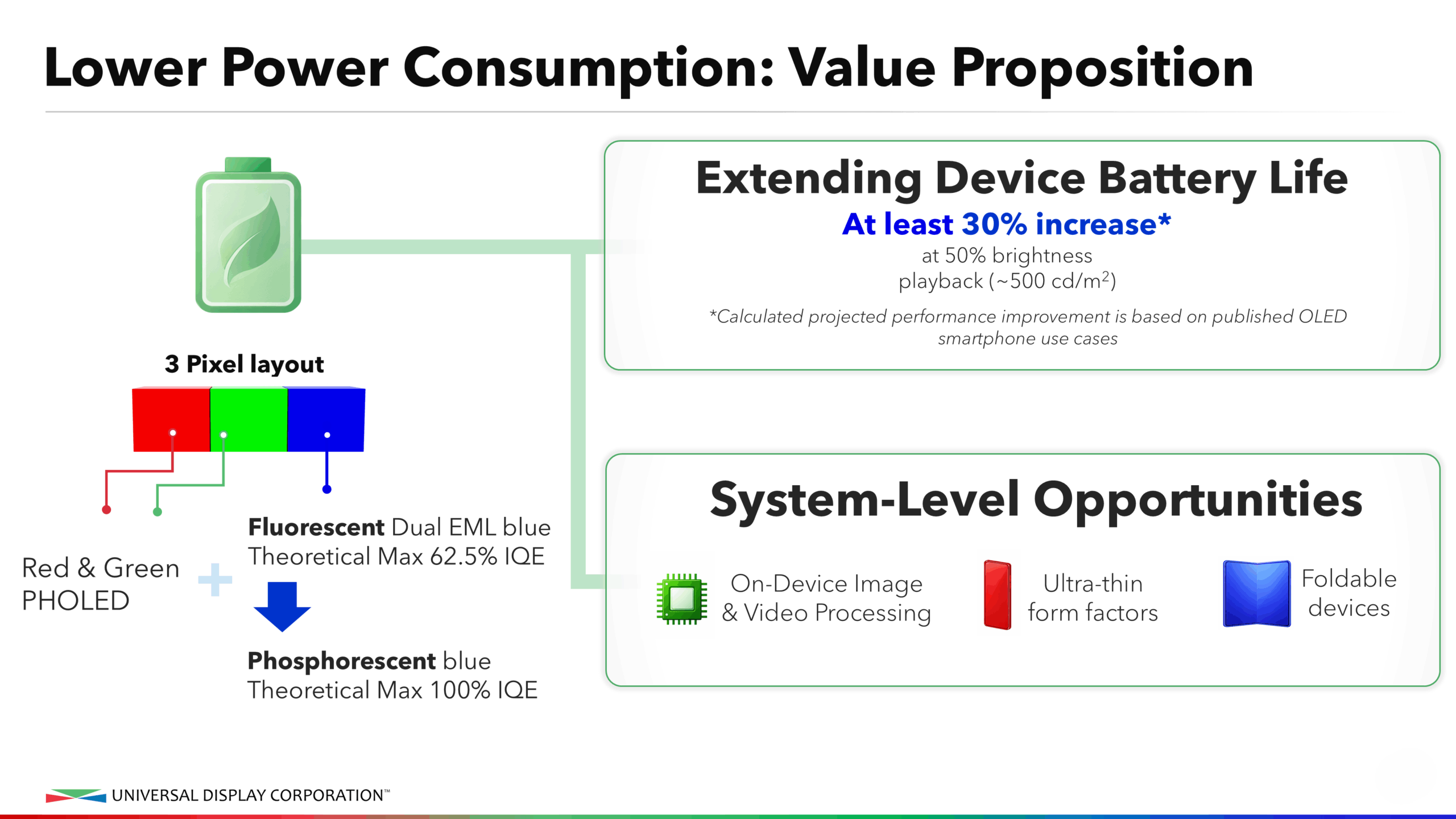
This opens up meaningful gains in panel efficiency. We estimate that replacing incumbent fluorescent blue technology with a phosphorescent blue emissive system in today’s single-stack OLED displays could deliver an entry-level increase in panel efficiency of up to approximately 25%, which can translate into:
- Lower power consumption
- Longer battery life
- Greater system-level design flexibility, allowing power savings from the display to be redirected toward processing, connectivity, or enhanced user experiences.
Q: UDC has been working on blue for years. Where are we now?
Fadi: What’s different today is that we’re seeing progress across multiple aspects of performance simultaneously, rather than isolated improvements.
In our recent work, we’ve demonstrated advances in:
- Efficiency – Improved external quantum efficiency (EQE)
- Color performance – Deeper, more saturated blue emission meeting BT.2020 color specifications
- Lifetime – Improved operational stability driven by increased intrinsic material stability and tailoring to specific use cases
- Material readiness – Enhanced phosphor thermal stability and the introduction of pre-mixed host systems, both critical for high-volume manufacturing
In earlier generations, progress in one area often came at the expense of another. Today, we’re achieving a more balanced performance profile across key requirements.
Q: Your presentation at SID Display Week highlighted multiple generations of blue materials. What’s the significance of that evolution?
Fadi: We’ve made significant progress at the molecular level that directly translates into improved device performance. For example, newer generations of materials demonstrate:
- Near-unity photoluminescent quantum yield (PLQY), enabling higher efficiency
- Narrower emission line shapes, supporting improved color purity
- Optimized frontier energy levels, enabling more effective integration with host materials and enhanced emissive layer stability.
When these materials are incorporated into devices, we observe:
- Deep, saturated blue colors
- Higher efficiency, reflected in improved EQE
- Lower operating voltage
- Improved operational stability
Taken together, these advances help address several of the key requirements for practical display applications.
Q: AI and machine learning were mentioned in your presentation. What role do they play?
Fadi: They play a significant role in accelerating materials discovery.
Traditionally, materials development relied heavily on experimentation and iterative trial-and-error. Today, AI and machine learning enable us to:
- Predict key material properties
- Model molecular behavior and optimize interactions within the emissive system
- Screen for new classes of emitters and hosts
These approaches operate at computational speeds orders of magnitude faster than traditional methods, helping to shorten development timelines. As a result, we can identify promising materials earlier and more efficiently deliver high-performance solutions aligned with the rapidly evolving demands of the OLED industry.
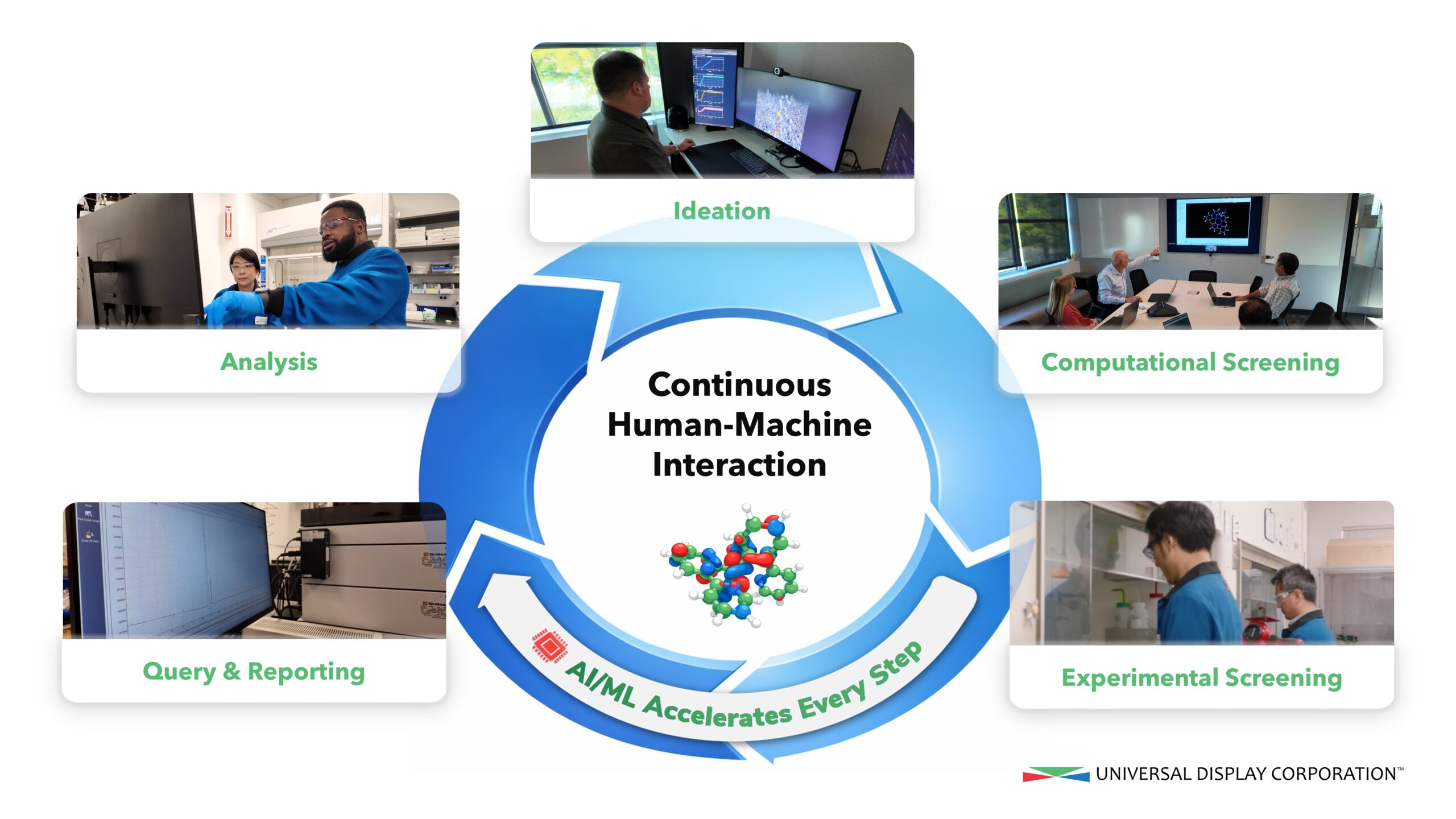
UDC’s AI-accelerated OLED innovation is defined by continuous human-machine interaction throughout discovery workflows.
Q: The concept of “architecture” comes up frequently. What does that mean?
Nick: In simple terms, architecture refers to how the OLED device is designed, meaning the structure and arrangement of its different layers.
What’s important is that blue phosphorescent materials are not limited to a single device design. They can be integrated into a range of architectures, including:
- Single-stack devices, the most widely used today, particularly in smartphones and wearables
- Tandem architectures, where multiple emissive layers are stacked to improve efficiency and lifetime, a direction the industry is increasingly pursuing for future IT and automotive products
- Hybrid approaches, such as phosphor-sensitized systems (PSF), which combine different material types to leverage their complementary properties.
This flexibility is important because it allows panel makers to adopt the technology in ways that align with their specific product and panel performance strategies.
Q: How do materials and architecture work together?
Fadi: They’re highly interdependent. Because phosphorescent materials enable 100% internal quantum efficiency, they directly enhance overall OLED panel efficiency, which in turn:
- Improves panel operational lifetime
- Reduces panel power consumption
When incorporated into advanced OLED architectures as the primary exciton harvesters, phosphorescent materials can further amplify device performance. For example, in tandem structures, the efficiency advantages of phosphorescent emitters become even more pronounced, as the benefits scale with each additional emissive layer.
This is why we often think about blue as part of an integrated system, where material innovation and device architecture work together to drive optimal performance.
Q: Beyond performance, what other factors are important?
Fadi: Performance alone is not sufficient. Materials must also meet a range of practical requirements.
For example, thermal stability is critical, as it directly determines a material’s ability to withstand high-rate deposition during mass production. In addition, many of the advanced architectures rely on multiple materials co-deposited within emissive layers, making the availability of pre-mixable host systems essential for simplifying the deposition process and accelerating technology adoption.
UDC has a long track record of meeting these requirements with our red, green, and yellow phosphorescent and host materials, and we are applying that same expertise to blue. For example:
- Designing phosphors to withstand extended exposure to elevated temperature stress under high-vacuum conditions consistent with mass production
- Developing high-performance pre-mixed host systems that simplify deposition and support more scalable manufacturing of advanced device architectures
These advances help bridge the gap between laboratory performance and manufacturing reality.
Q: Final question: How would you summarize where things stand today?
Nick: Blue phosphorescence has long been one of the most complex challenges in OLED technology, and at the same time, one of its most important opportunities.
What’s especially exciting today is not just the progress itself, but how that progress is coming together. We’re now seeing advances in materials design, device performance, and architecture come together in a much more coordinated way.
As the industry continues to push toward higher performance and lower power consumption, it’s becoming increasingly clear that achieving high-efficiency blue will require innovation across the entire system, from the emissive materials through to the device stack and manufacturing process.
That’s where we’ve been investing for many years. As these pieces come together, we believe we are well positioned to help enable that next phase of OLED innovation.
This progress also points to a broader opportunity as the technology continues to evolve. Blue complements today’s well-established phosphorescent emissive layers, while offering a meaningful path to further improving display power efficiency. Over time, we expect high-efficiency blue adoption to approach the scale we see with green today, giving OLED displays a continued path to lower power consumption and enabling richer, more feature-enabled user experiences.
 |
Dr. Nick ThompsonNicholas Thompson is a R&D Director of New Tech Commercialization at Universal Display Corporation, where he works at the intersection of OLED research, technology development, and future display applications. His work focuses on advancing high-efficiency OLED technologies including blue phosphorescent OLEDs and plasmonic PHOLED device architectures. Dr. Thompson earned his Ph.D. in Materials Science and Engineering from MIT under Professor Marc Baldo and has spent more than two decades working on organic materials and device innovation. At UDC, his work supports the Company’s broader mission to enable energy-efficient OLED displays through innovation in emissive materials, device architectures, and new technologies. |
 |
Dr. Fadi JradiFadi M. Jradi is a Senior Research Scientist at Universal Display Corporation, where he is focused on the development and commercialization of high-efficiency phosphorescent blue OLED materials and technologies. He works closely with partners to support and guide key programs spanning early-staged material design through panel development and integration. Prior to joining UDC, Dr. Jradi completed a postdoctoral fellowship at the Howard Hughes Medical Institute, where he developed fluorescent probes for optical super-resolution microscopy. He holds a Ph.D. in Chemistry from the Georgia Institute of Technology under Professor Seth R. Marder, as well as M.S. and B.S. degrees in Chemistry from the American University of Beirut. |
Statements in this blog that are not historical facts are forward-looking statements. These statements involve risks and uncertainties that could cause actual results to differ materially. We undertake no obligation to update these statements. For more information, please view this website’s Legal Terms of Use under the ‘Safe Harbor’ heading.”

